Display Board Building
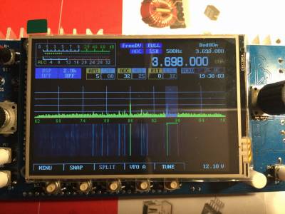
3.5" is the OVI40-SDR standard default display
The 3.5 inch LCD panel has exactly the same outer dimensions as the PCB porting plate of the previous 3.2 inch display. The key switches S7 and S8 on the UI board need to be mounted in the “lower” positions (i.e. in line with the function keys below LCD), in order not to be in the way.
Display Board
The display board plugs into UI board vonnector directly. The display board contains LCD display and touch panel functionality. For mechanical mounting oDie Displayplatine beinhaltet Display und Touchpanel. For mechanical mounting considerations please see below.
The following LCDs can be used with UI board V1.8 and UHSDR:
- 3.5“ display 480×320 with controller ILI9846 (ot ILI9846 compatible controller): OVI40 default display
- 3.2” display 320 x 240 witch controller IL9325 (or IL9325 compatible controller): this was the display used during UI V1.8 beta testing
- 2.8“ display 320 x 240 with controller IL9325 (or compatible controller): this is the mcHF defult display
Display Calibration - mandatory at first bring-up
Important: It is mandatory to do a display calibration at first bring-up / switch on of the touch screen display. Only after calibration will the touch screen work with UHSDR.
Start the calibration by touching the touch screen with a finger before switching on the UI board V1.8. Keep touching the touch screen until the service menu sis displayed. Now release the finger from the touch screen and follow instructions on the screen carefully. After calibration is finished please leave the test screen by pressing the POWER button and then, when firmware start to work, please long press MENU (F1) button to save the calibration settings (the MENU should be marked with * and different colour, which means you have not saved settings).
Sometimes calibration fails and there is need to repeat it. That's why there is a test screen with drawing dots (you can use also the blue test screen to check if it works). You have to play with it to be familiar. If the accuracy is not perfect (it should be less than 1mm) you have to change the calibration method or have issue with the panel itself. One preferred method for calibration is to use plastic stylus or soft pencil (gentle), but you can do it with nail with good results.
Mechanical fixing of the display board onto the UI board
The display board will be mechanically held in position by the casing. As long as the casing is not available yet, a temporary solution is required.
Simple approach: a piece of non-conductive material (e.g. plastic) of suitable height can be fixed between UI board and LCD PCB with double-sided self-adhesive tape. This will keep the display board stabilized and away from the UI board.
Just make sure that it is still possible to easy unplugging of the display board is still possible, when needed.
Alternatively plastic spacer bolts may be used:
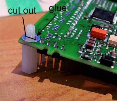
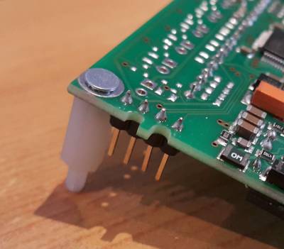
Option 1 plastic spacer Plastik-Abstandshalter with inner thread and outer thread, e.g. https://www.tme.eu/pl/details/tp-11/tuleje-dystansowe-plastikowe/fixfasten/. Please refer to photo below: the outher thread is cut flush with the display PCB board, then glued. The spacer bolt is fixed onto the UI board with adhesive tape.
Option 2 plastic spacer bolt with two inner threads, e.g. https://www.tme.eu/pl/details/hp-10/tuleje-dystansowe-plastikowe/fixfasten/. This spacer bolt is fixed with display PCB by screw and fixed to UI PCB by adhesive tape.
Display Brightness
The LCD display brightness can be adjusted by changing R105 (15 Ohm default) to a different vlue. R105 is next to the SOIC8-IC
According to LCD data sheet the maximum DC current allowed is 60 mA continous, or 75 mA for less than a minute. When changing R105 please make sure not to exceed 60 mA.
Reducing R105 to 10 Ohm typically allows to increas brightness (if needed) while staying within specifications.
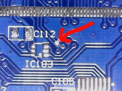
Cutting SDO line
Note: It is necessary to cut the SDO line for all LCD display boards delivere befor January 5, 2018. Displays delivered later have this modification already.
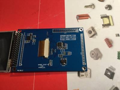
Pleae cut the PCB trace as shown in photo. This is the SPI SDO “data output” line from display. This line does not go tri-state in tri-state mode. It needs to be cut so that the tuch screen controller ADS8743 / TSC2046 can not be detected by UI board MCU Display.
Display Assembly
Note: The display board is delivered as an assembled and tested unit. Explanations below refer to self-assembly, not required, and are added for completeness and reference only
This pdf contains th modified assembly notes: lcd_35_40pin_df8oe_sp9bsl.pdf
- C103, C112, IC103 and R106 are not needed anymore
- R101 = R104 = 100K
- R102 = 15R
- R105 = 3.3R
- all 10u now replaced by 1u
- XPT2046 = ADS7843E
Put a small wire between pin3 and pin4 of IC103. Shorten R107 forever.
LCD can only work in parallel mode - there will never be a SPI mode.
DF8OE suggest to replace the two parallel tantal capacitors next to the 3.3V voltage regulator by 100nF & 1uF. He also suggest to put 100nF & 1uF in the free location shown in Andy's photo.
The two pads of R107 location need to be short cut, otherwise the LCD won't work.
Only LCD parallel mode is supported at this time.
Possitioning the LCD on the PCB
The lower left corner of the LCD should be flush with the PCB.
Dazu die LCD links unten ansetzen und sie bei bereits eingestecktem Flachkabel vorsichtig in Richtung PCB umklappen. Irgendwann geht es schwerer - weil das Flachkabel jetzt zwischen LCD und PCB Wellen schlägt. Nun auf der Seite der PCB mit dem FPC mit einem Schraubendreher zwischen Flachkabel und PCB gehen und vorsichtig eine kleine Schlaufe rausziehen. Das LCD klappt nun wie von selbst gegen die PCB und kann vorsichtig (!!) am linken, oberen und unteren Rand angedrückt werden.
Das Doppelklebeband links in voller Höhe (überdeckt die 20pol Löcher) in ca. 1cm Breite positionieren, und dann oben und unten in ca. 5mm Breite über die volle PCB Länge. Rechts kommt KEIN Klebeband hin. Es ist zu vermeiden rechts mit Kraft auf das LCD zu drücken. Dort ist es sehr empfindlich, weil dort kein Plastik-Rand darunter ist.
On shortening the male header J103 on OVI40 UI for LCD display
Cutting the male header pins pf J103 (on component side) is required to reduce height of the LCD Display module above OVI40 UI PCB. Cutting / shortening the pins on component side might not be the best idea as it damages the female connector each time it's inserted, due to the fact that cutting the J103 pins produces sharp edges that scratch the femaile LCD display header.
An alternative is to solder the pins at the right depth and then cut the pins flush to the pcb on the solder side.
